Fermi Level In Semiconductor - Fermi Level Pinning Explained A M S Contact Where The Fermi Level Is Download Scientific Diagram / Equation 1 can be modied for an intrinsic semiconductor, where the fermi level is close to center of the band gap (ef i).
Fermi Level In Semiconductor - Fermi Level Pinning Explained A M S Contact Where The Fermi Level Is Download Scientific Diagram / Equation 1 can be modied for an intrinsic semiconductor, where the fermi level is close to center of the band gap (ef i).. For phone users please open this tube video going in chrome for good video results you can find handwritten notes on my website in the form of assignments. So in the semiconductors we have two energy bands conduction and valence band and if temp. Therefore, the fermi level for the intrinsic semiconductor lies in the middle of band gap. The fermi level (i.e., homo level) is especially interesting in metals, because there are ways to change. Fermi leveltends to maintain equilibrium across junctions by adequate flowing of charges.
Thus, electrons have to be accommodated at higher energy levels. Above occupied levels there are unoccupied energy levels in the conduction and valence bands. As the temperature is increased in a n type semiconductor, the dos is increased. The fermi level is on the order of electron volts (e.g., 7 ev for copper), whereas the thermal energy kt is only about 0.026 ev at 300k. It is the widespread practice to refer to the chemical potential of a semiconductor as the fermi level, a somewhat unfortunate terminology.
Work Function Wikiwand from upload.wikimedia.org In all cases, the position was essentially independent of the metal. Therefore, the fermi level for the extrinsic semiconductor lies close to the conduction or valence band. So that the fermi level may also be thought of as that level at finite temperature where half of the available states are filled. It is a thermodynamic quantity usually denoted by µ or ef for brevity. Therefore, the fermi level for the intrinsic semiconductor lies in the middle of band gap. Thus, electrons have to be accommodated at higher energy levels. Fermi level is also defined as the. The fermi level is the surface of fermi sea at absolute zero where no electrons will have enough energy to rise above the surface.
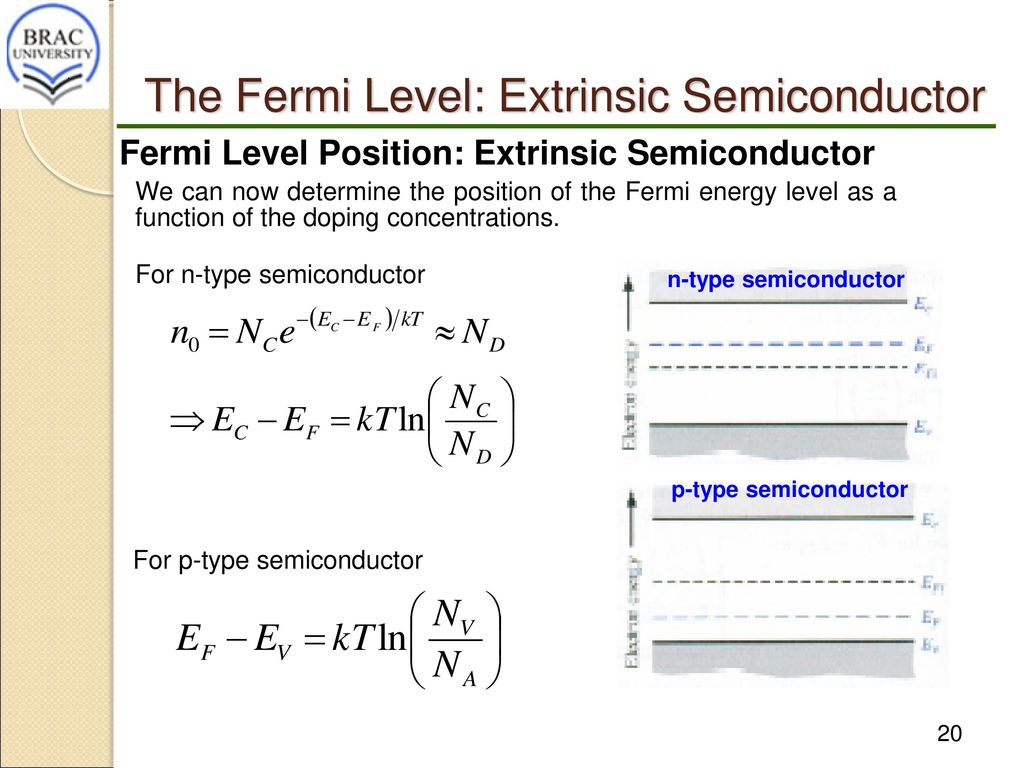
Therefore, the fermi level for the extrinsic semiconductor lies close to the conduction or valence band.
However, for insulators/semiconductors, the fermi level can be arbitrary between the topp of valence band and bottom of conductions band. Increases the fermi level should increase, is that. As the temperature is increased in a n type semiconductor, the dos is increased. Uniform electric field on uniform sample 2. • the fermi function and the fermi level. The fermi level does not include the work required to remove the electron from wherever it came from. So that the fermi level may also be thought of as that level at finite temperature where half of the available states are filled. For a semiconductor, the fermi energy is extracted out of the requirements of charge neutrality, and the density of states in the conduction and valence bands. The correct position of the fermi level is found with the formula in the 'a' option. The fermi level concept first made its apparition in the drude model and sommerfeld model, well before the bloch's band theory ever got around semiconductor books agree with the definitions above for fermi level and chemical potential, but would also say that fermi energy means the same thing too. The occupancy of semiconductor energy levels. Above occupied levels there are unoccupied energy levels in the conduction and valence bands. Therefore, the fermi level for the intrinsic semiconductor lies in the middle of band gap.
• the fermi function and the fermi level. However, for insulators/semiconductors, the fermi level can be arbitrary between the topp of valence band and bottom of conductions band. Thus, electrons have to be accommodated at higher energy levels. It is well estblished for metallic systems. The band theory of solids gives the picture that there is a sizable gap between the fermi level and the conduction band of the semiconductor.
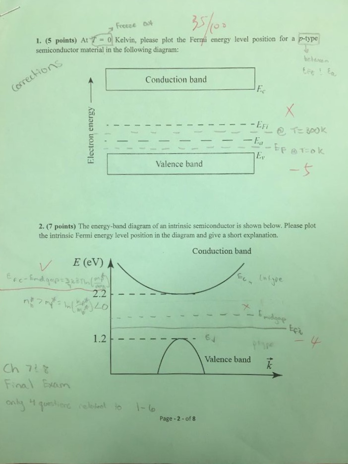
Solved Frence Of 1 5 Points At Kelvin Please Plot The Chegg Com from d2vlcm61l7u1fs.cloudfront.net Position is directly proportional to the logarithm of donor or acceptor concentration it is given by in either material, the shift of fermi level from the central. Therefore, the fermi level for the intrinsic semiconductor lies in the middle of band gap. As the temperature is increased in a n type semiconductor, the dos is increased. Uniform electric field on uniform sample 2. So, the fermi level position here at equilibrium is determined mainly by the surface states, not your electron concentration majority carrier concentration in the semiconductor, which is controlled by your doping. The fermi level is on the order of electron volts (e.g., 7 ev for copper), whereas the thermal energy kt is only about 0.026 ev at 300k. The fermi level is on the order of electron volts (e.g., 7 ev for copper), whereas the thermal energy kt is only about 0.026 ev at 300k.
The topic is not so easy to understand and explain.
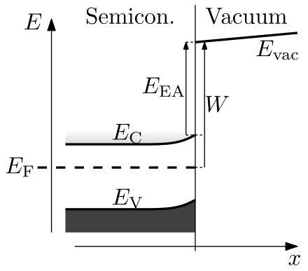
In simple term, the fermi level signifies the probability of occupation of energy levels in conduction band and valence band. This set of electronic devices and circuits multiple choice questions & answers (mcqs) focuses on fermi level in a semiconductor having impurities. Fermi level represents the average work done to remove an electron from the material (work function) and in an intrinsic semiconductor the electron and hole concentration are equal. Where will be the position of the fermi. The occupancy of semiconductor energy levels. Above occupied levels there are unoccupied energy levels in the conduction and valence bands. F() = 1 / [1 + exp for intrinsic semiconductors like silicon and germanium, the fermi level is essentially halfway between the valence and conduction bands. Main purpose of this website is to help the public to learn some. at any temperature t > 0k. The topic is not so easy to understand and explain. Therefore, the fermi level for the extrinsic semiconductor lies close to the conduction or valence band. Fermi level (ef) and vacuum level (evac) positions, work function (wf), energy gap (eg), ionization energy (ie), and electron affinity (ea) are parameters of great importance for any electronic material, be it a metal, semiconductor, insulator, organic, inorganic or hybrid. In all cases, the position was essentially independent of the metal.
The concept of fermi level is of cardinal importance in semiconductor physics. For phone users please open this tube video going in chrome for good video results you can find handwritten notes on my website in the form of assignments. Fermi statistics, charge carrier concentrations, dopants. It is well estblished for metallic systems. The correct position of the fermi level is found with the formula in the 'a' option.
Eee209 Ece230 Semiconductor Devices And Materials Ppt Video Online Download from slideplayer.com If so, give us a like in the sidebar. The fermi level does not include the work required to remove the electron from wherever it came from. The illustration below shows the implications of the fermi function for the electrical conductivity of a semiconductor. Increases the fermi level should increase, is that. Position is directly proportional to the logarithm of donor or acceptor concentration it is given by However, for insulators/semiconductors, the fermi level can be arbitrary between the topp of valence band and bottom of conductions band. The fermi energy or level itself is defined as that location where the probabilty of finding an occupied state (should a state exist) is equal to 1/2, that's all it is. Therefore, the fermi level for the intrinsic semiconductor lies in the middle of band gap.
Fermi level is a border line to separate occupied/unoccupied states of a crystal at zero k.
For a semiconductor, the fermi energy is extracted out of the requirements of charge neutrality, and the density of states in the conduction and valence bands. If so, give us a like in the sidebar. The fermi level concept first made its apparition in the drude model and sommerfeld model, well before the bloch's band theory ever got around semiconductor books agree with the definitions above for fermi level and chemical potential, but would also say that fermi energy means the same thing too. Increases the fermi level should increase, is that. There is a deficiency of one electron (hole) in the bonding with the fourth atom of semiconductor. Thus, electrons have to be accommodated at higher energy levels. Uniform electric field on uniform sample 2. It is well estblished for metallic systems. Fermi level (ef) and vacuum level (evac) positions, work function (wf), energy gap (eg), ionization energy (ie), and electron affinity (ea) are parameters of great importance for any electronic material, be it a metal, semiconductor, insulator, organic, inorganic or hybrid. The band theory of solids gives the picture that there is a sizable gap between the fermi level and the conduction band of the semiconductor. Main purpose of this website is to help the public to learn some. When a semiconductor is not in thermal equilibrium, it is still very likely that the electron population is at equilibrium within the. It is a thermodynamic quantity usually denoted by µ or ef for brevity.


0 Komentar